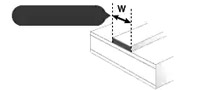
PCB Trace Width Calculator
A
About
This tool uses formulas from IPC-2221 to calculate the width of a copper printed circuit board conductor or "trace" required to carry a given current while keeping the resulting increase in trace temperature below a specified limit. If the length of the trace is also provided, the total resistance, voltage drop, and power loss due to trace resistance are also calculated. The results are estimates; actual results may vary depending on application conditions. Note also that required widths are significantly higher for traces on internal layers of a circuit board compared to those on a board’s outer surface; use whichever result is appropriate for your situation.
How to Calculate Trace Width:
First, calculate the Area:
Area[mils^2] = (Current[Amps]/(k*(Temp_Rise[deg. C])^b))^(1/c)
Then, calculate the Width:
Width[mils] = Area[mils^2]/(Thickness[oz]*1.378[mils/oz])
For IPC-2221 internal layers: k = 0.024, b = 0.44, c = 0.725
For IPC-2221 external layers: k = 0.048, b = 0.44, c = 0.725
where k, b, and c are constants resulting from curve fitting to the IPC-2221 curves.
Common values:
Thickness: 1 oz
Ambient: 25 C
Temp rise: 10 C
Minimum Printed Line Width
Lnner Layer
Required Printed Line Width
Resistance (Ω)
Voltage Drop (V)
Power Loss (W)
Minimum Printed Line Width
Bare Outer Layer
Required Printed Line Width
Resistance (Ω)
Voltage Drop (V)
Power Loss (W)